- 您现在的位置:买卖IC网 > Sheet目录3882 > PIC24F08KL301-I/SS (Microchip Technology)IC MCU 16BIT 8KB FLASH 20-SSOP
CHAPTER 5 BUS CONTROL FUNCTION
User’s Manual U15905EJ2V1UD
178
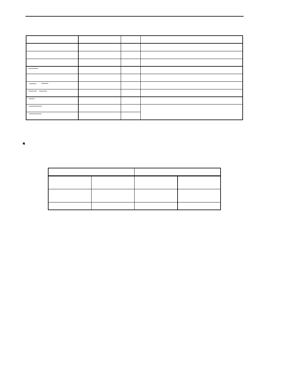
Table 5-2. External Control Pins (Separate Bus)
Bus Control Pin
Alternate-Function Pin
I/O
Function
AD0 to AD15
PDL0 to PDL15
I/O
Data bus
A0 to A15
P90 to P915
Output
Address bus
A16 to A23
Note
PDH0 to PDH7
Output
Address bus
WAIT
PCM0
Input
External wait control
CLKOUT
PCM1
Output
Internal system clock
CS0 to CS3
PCS0 to PCS3
Output
Chip select
WR0, WR1
PCT0, PCT1
Output
Write strobe signal
RD
PCT4
Output
Read strobe signal
HLDRQ
PCM3
Input
HLDAK
PCM2
Output
Bus hold control
Note
A16 to A21 in the V850ES/SA2
5.2.1
Pin status when internal ROM, internal RAM, or internal peripheral I/O is accessed
When the internal ROM, internal RAM, or internal peripheral I/O is accessed, the status of each pin is as follows.
Table 5-3. Pin Status When Internal ROM, Internal RAM, or Internal Peripheral I/O Is Accessed
Separate Mode
Multiplexed Bus Mode
Address bus
(A23 to A0)
Undefined
Address bus
(A23 to A16)
Undefined
Data bus
(AD15 to AD0)
Hi-Z
Data bus
(AD15 to AD0)
Undefined
Control signal
Inactive
Control signal
Inactive
Caution
When the internal ROM area is write-accessed, the addresses, data, and control signals
are activated in the same way as access to the external memory area.
5.2.2
Pin status in each operation mode
For the pin status of the V850ES/SA2 and V850ES/SA3 in each operation mode, refer to 2.2 Pin Status.
发布紧急采购,3分钟左右您将得到回复。
相关PDF资料
PIC18LF1220T-I/ML
IC MCU FLASH 2KX16 EEPROM 28QFN
PIC18LF1220T-I/SO
IC MCU FLASH 2KX16 EEPROM 18SOIC
PIC16F716-I/SS
IC PIC MCU FLASH 2KX14 20SSOP
PIC18F1320T-E/ML
IC MCU FLASH 4KX16 EEPROM 28QFN
PIC16LF87T-I/ML
IC MCU FLASH 4KX14 EEPROM 28QFN
PIC18F25J10-I/SS
IC PIC MCU FLASH 16KX16 28SSOP
PIC16F88T-E/SS
IC MCU FLASH 4KX14 EEPROM 20SSOP
PIC16C621A-04/SO
IC MCU OTP 1KX14 COMP 18SOIC
相关代理商/技术参数
PIC24F08KL301T-I/MQ
功能描述:16位微控制器 - MCU 8KB FLASH 1KB RAM 512B 3V 10-BIT ADC RoHS:否 制造商:Texas Instruments 核心:RISC 处理器系列:MSP430FR572x 数据总线宽度:16 bit 最大时钟频率:24 MHz 程序存储器大小:8 KB 数据 RAM 大小:1 KB 片上 ADC:Yes 工作电源电压:2 V to 3.6 V 工作温度范围:- 40 C to + 85 C 封装 / 箱体:VQFN-40 安装风格:SMD/SMT
PIC24F08KL301T-I/SO
功能描述:16位微控制器 - MCU 8KB FLASH 1KB RAM 512B 3V 10-BIT ADC RoHS:否 制造商:Texas Instruments 核心:RISC 处理器系列:MSP430FR572x 数据总线宽度:16 bit 最大时钟频率:24 MHz 程序存储器大小:8 KB 数据 RAM 大小:1 KB 片上 ADC:Yes 工作电源电压:2 V to 3.6 V 工作温度范围:- 40 C to + 85 C 封装 / 箱体:VQFN-40 安装风格:SMD/SMT
PIC24F08KL301T-I/SS
功能描述:16位微控制器 - MCU 8KB FLASH 1KB RAM 512B 3V 10-BIT ADC RoHS:否 制造商:Texas Instruments 核心:RISC 处理器系列:MSP430FR572x 数据总线宽度:16 bit 最大时钟频率:24 MHz 程序存储器大小:8 KB 数据 RAM 大小:1 KB 片上 ADC:Yes 工作电源电压:2 V to 3.6 V 工作温度范围:- 40 C to + 85 C 封装 / 箱体:VQFN-40 安装风格:SMD/SMT
PIC24F08KL302
制造商:MICROCHIP 制造商全称:Microchip Technology 功能描述:Low-Power, Low-Cost, General Purpose 16-Bit Flash Microcontrollers with nanoWatt XLP Technology
PIC24F08KL302-I/ML
功能描述:16位微控制器 - MCU 8KB FLASH 1KB RAM 256B 3V RoHS:否 制造商:Texas Instruments 核心:RISC 处理器系列:MSP430FR572x 数据总线宽度:16 bit 最大时钟频率:24 MHz 程序存储器大小:8 KB 数据 RAM 大小:1 KB 片上 ADC:Yes 工作电源电压:2 V to 3.6 V 工作温度范围:- 40 C to + 85 C 封装 / 箱体:VQFN-40 安装风格:SMD/SMT
PIC24F08KL302-I/MQ
功能描述:16位微控制器 - MCU 8KB FL 1KB RAM 256B 3V RoHS:否 制造商:Texas Instruments 核心:RISC 处理器系列:MSP430FR572x 数据总线宽度:16 bit 最大时钟频率:24 MHz 程序存储器大小:8 KB 数据 RAM 大小:1 KB 片上 ADC:Yes 工作电源电压:2 V to 3.6 V 工作温度范围:- 40 C to + 85 C 封装 / 箱体:VQFN-40 安装风格:SMD/SMT
PIC24F08KL302-I/SO
功能描述:16位微控制器 - MCU 8KB FLASH 1KB RAM 256B 3V RoHS:否 制造商:Texas Instruments 核心:RISC 处理器系列:MSP430FR572x 数据总线宽度:16 bit 最大时钟频率:24 MHz 程序存储器大小:8 KB 数据 RAM 大小:1 KB 片上 ADC:Yes 工作电源电压:2 V to 3.6 V 工作温度范围:- 40 C to + 85 C 封装 / 箱体:VQFN-40 安装风格:SMD/SMT
PIC24F08KL302-I/SP
功能描述:16位微控制器 - MCU 8KB FLASH 1KB RAM 256B 3V RoHS:否 制造商:Texas Instruments 核心:RISC 处理器系列:MSP430FR572x 数据总线宽度:16 bit 最大时钟频率:24 MHz 程序存储器大小:8 KB 数据 RAM 大小:1 KB 片上 ADC:Yes 工作电源电压:2 V to 3.6 V 工作温度范围:- 40 C to + 85 C 封装 / 箱体:VQFN-40 安装风格:SMD/SMT